UNDERSTANDING THE BASIS OF SEMICONDUCTORS
In my previous article, I explained some basic terms known with semiconductors. I was able to stop at the classification of semiconductors into N-type and P-type based on their intrinsic behaviours. Today, I will start by explaining what these two types of semiconductors really are.
Check the previous article here
N-TYPE SEMICONDUCTOR
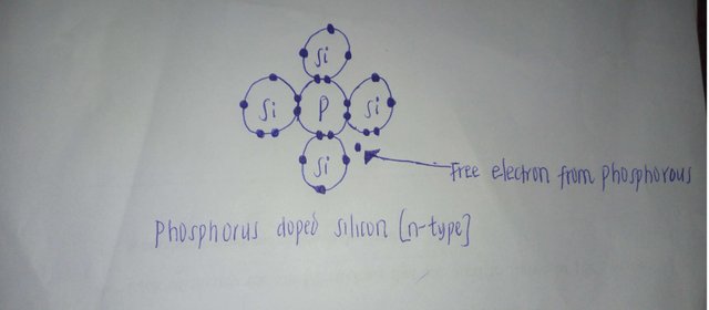
Certain elements such as phosphorus, antimony and arsenic are pentavalent i.e. each atom has five valence electrons. An N-type semiconductor is formed when an intrinsic material is doped with atoms of pentavalent element. The pentavalent atom shares four of its five valence electrons with adjacent atoms but the fifth electron is not tightly bound to its parent atom and is free to facilitate flow of current through the material.
After ionization, the positive charges (protons) contained in the donor atoms are tightly bound in the crystal lattice while the electrons move freely in the material hence the electrons are called mobile charges. Also, the conduction band electrons outnumber the thermally generated holes by many orders of magnitude thus the electrons in the N-type materials are referred to as the majority carriers while the few thermally generated holes are called minority carriers.
Source: @thestronics
P-TYPE SEMICONDUCTOR
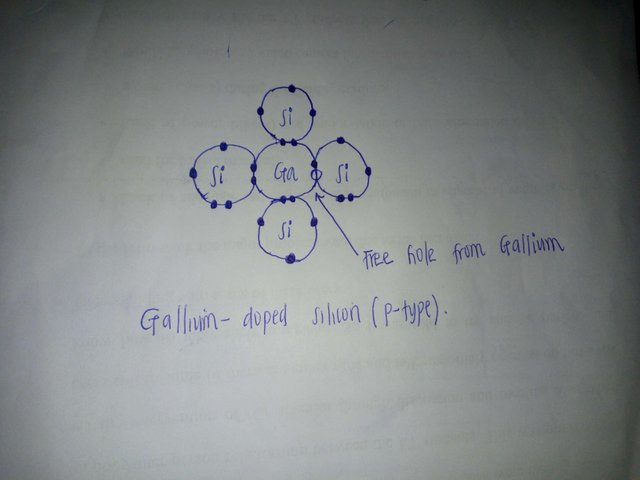
Materials such as gallium, indium, boron, aluminum are trivalent i.e. each atom has only three valence electrons. A P-type semiconductor is formed when an intrinsic material is doped with atoms of trivalent element called acceptor atoms. Each trivalent atom forms three covalent bonds with the neighboring silicon atoms thereby creating a whole where the fourth bond is supposes to be.
After ionization, the electrons are tightly bound in the crystal lattice while the holes move freely in the material. Hence, in a P-type material, the bounded electrons are the immobile carriers while the holes are the mobile carriers. Also, the concentration of holes in the valence band is much greater than the concentration of electrons in the conduction band. Consequently, in a P-type materials, holes are the majority carriers while the few thermally generated electrons are the minority carriers.
Source: @thestronics
Let Nd = concentration of donor atoms
Na = concentration of acceptor atoms
n = concentration of electrons in the conduction band
p = concentration of holes in the valence band
Assuming 100% ionization, then by the law of electrical neutrality:
Nd + p = Na + n
Also, by the law of mass action;
np = n²i
It should be noted that mass action laws hold for both intrinsic and extrinsic semiconductors. Take for instance, in an n-type material, the mass action law is given by:
(Pn)(Nn) = n²i (the subscript ‘n’ indicates an n-type material.
Where Pn = concentration of thermally generated holes in the valance band.
Nn = total concentration of electrons in the conduction band.
NOTE: For every thermally generated holes, there must be a corresponding thermally generated electrons.
If Nn is approximately equals to Nd:
Then Pn = (n²i)/ Nd
Similarly Np = (n²i)/Na
P-N JUNCTION UNDER ZERO BIAS
A p-n junction is formed if there is an abrupt change from a p-doped region to an n-doped region within the semiconductor material. The p-type region of the diode is known as the anode (A) while the n-type region is called the cathode (K). If we have not forgotten, an n-type material has a large concentration of electrons and few thermally generated holes whereas in a p-type material, there is large concentrations of holes and few thermally generated electrons.
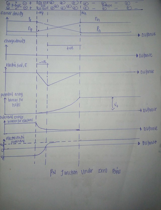
As soon as the junction is formed, carrier concentration gradients are formed such that the holes diffuse from the p-side to the n-side while the electrons diffuse from the n-side to the p-side. When the holes reach the n-side, they recombine with the free electrons. Similarly, electrons diffusing into the p-side recombines with the free holes in the p-side. Consequently, an area is created on the either side of the junction that is depleted of free charges. This region is called the depletion region.
Now as the mobile majority carriers in the p-type materials (holes) migrate across the junction, they leave behind them immobile negative charges. This has the effect of making the depletion region in the p-side to become negatively charged. A similar situation causes the depletion region in the n-side to become positively charged. All these explanations are shown in the figure below:
Source: @thestronics
The positively charged depletion region in the n-side constitutes a potential energy barrier against the further diffusion of holes across the junctions as shown above. Similarly, the negatively charged depletion region in the p-side constitutes a potential barrier against further diffusion of electrons as shown in the figure above.
BIASED P-N JUNCTION
FORWARD BIAS:
Source: @thestronics
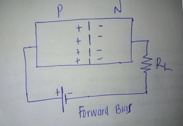
A p-n junction is said to be forward biased when a DC voltage source with an electromotive force greater than the barrier potential difference is connected with its positive terminal to the anode (A) and its negative terminal to the cathode (K).
This causes the majority carriers to be repelled by the source terminals towards the junctions i.e. electrons which are majority carriers in the n-side (cathode) are repelled towards the junction by the negative terminals while the holes which are the majority carriers in the p-side (anode) are repelled towards the junction by the positive terminal.
The effect of this is that there is recombination of the majority at this junction which results into flow of current in the forward direction. A small increase in the applied voltage in the forward direction results in an exponential increase in the current due to the reduction of the potential barrier.
REVERSE BIAS:
Source: @thestronics
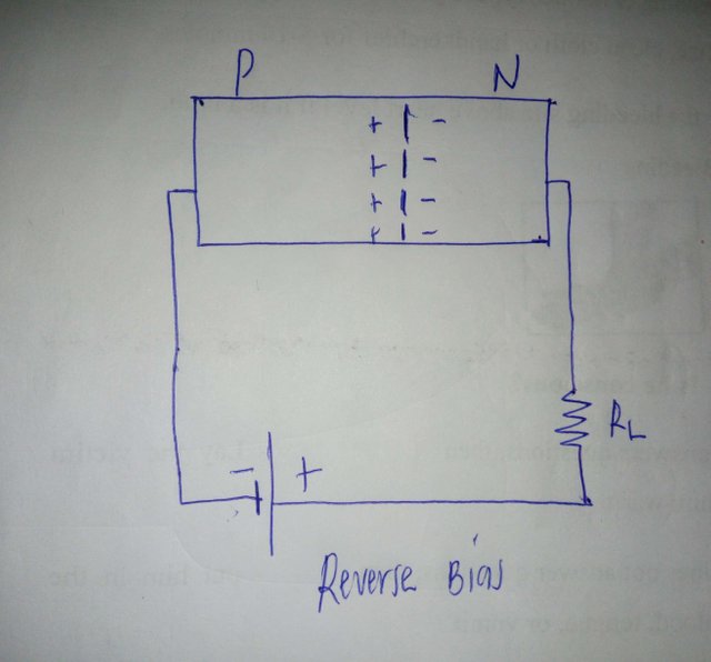
Under reverse bias condition, the negative terminal of the DC voltage is connected to the anode (A) and the positive terminal to the cathode (K).Under this condition, the majority carriers in the p-region (holes) are attracted by the negative terminal of the voltage source while the electron (majority carriers in the n-region) are attracted by the positive terminal of the source such that the depletion region wide and the barrier potential difference is reinforced.
Since the majority carriers are not crossing the junction, there is no flow of current in the forward direction. However, as a result of recombination of the thermally generated minority carriers at the junction, a small reverse saturation current, Is, increases with increasing reverse bias until the breakdown voltage Vbd is reached when there is sudden flow of large current. With the exception of Zener diode, all other diode gets destroyed when operated in the breakdown region.
Since the minority carriers are thermally generated, the magnitude of reverse saturation current is a function of the temperature of the semiconductor and the applied reverse bias.
THANKS FOR TAKING YOUR TIME TO READ!!!
REFERENCES

Being A SteemStem Member
Hi! I am a robot. I just upvoted you! I found similar content that readers might be interested in:
https://en.wikipedia.org/wiki/P%E2%80%93n_junction
@cheetah needs to go school.